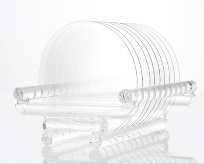
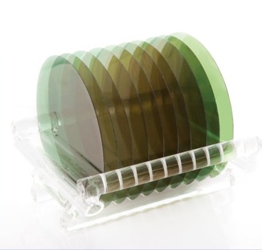
產品示意
6英吋 SIC wafer
4英吋 SIC wafer
4 英寸高純半絕緣 4H-SiC Substrate(Production Grade)
| Parameter | Value |
|---|---|
| Diameter | 99.5 ~ 100 mm |
| Thickness | 500 ± 25 μm |
| Resistivity | ≥ 1E9 ohm·cm |
| Micro-pipe Density | ≤ 0.5 ea/cm² |
| TTV | ≤ 5 μm |
| LTV | ≤ 2 μm (5mm × 5mm) |
| Bow | -15 μm ~ 15 μm |
| Warp | ≤ 20 μm |
| Roughness | ≤ 0.2 nm (5μm × 5μm) |
| Note | Research & Dummy Grade is also available. Please consult to your sales. |
6 英寸高純半絕緣 4H-SiC Substrate(Production Grade)
| Parameter | Value |
|---|---|
| Diameter | 150 ± 0.2 mm |
| Thickness | 500 ± 25 μm |
| Primary flat orientation | [1-100] ± 5° or Notch |
| Resistivity | ≥ 1E8 ohm·cm |
| Micro-pipe Density | ≤ 0.5 ea/cm² |
| TTV | ≤ 3 μm (5mm × 5mm) |
| LTV | ≤ 5 μm |
| Bow | -25 μm ~ 25 μm |
| Warp | ≤ 35 μm |
| Roughness | ≤ 0.2 nm (5μm × 5μm) |
| Note | Research & Dummy Grade is also available. Please consult to your sales. |
4 英寸 N 型 4H-SiC Substrate(Production Grade)
| Parameter | Value |
|---|---|
| Diameter | 99.5 ~ 100 mm |
| Thickness | 350 ± 25 μm |
| Resistivity | 0.015 ~ 0.025 ohm·cm |
| Micro-pipe Density | ≤ 0.5 ea/cm² |
| TTV | ≤ 2 μm (5mm × 5mm) |
| LTV | ≤ 5 μm |
| Bow | -15 μm ~ 15 μm |
| Warp | ≤ 20 μm |
| Roughness | ≤ 0.2 nm (5μm × 5μm) |
| Note | Research & Dummy Grade is also available. Please consult to your sales. |
6 英寸 N 型 4H-SiC Substrate(Production Grade)
| Parameter | Value |
|---|---|
| Diameter | 150.0 ± 0.2 mm |
| Thickness | 350 ± 25 μm |
| Resistivity | 0.015 ~ 0.025 ohm·cm |
| Micro-pipe Density | ≤ 0.5 ea/cm² |
| TTV | ≤ 3 μm (5mm × 5mm) |
| LTV | ≤ 5 μm |
| Bow | -25 μm ~ 25 μm |
| Warp | ≤ 35 μm |
| Roughness | ≤ 0.2 nm (5μm × 5μm) |
| Note | Research & Dummy Grade is also available. Please consult to your sales. |
6 英寸 N 型 4H-SiC N-type Epitaxial Wafer(Specification 650V)
Epitaxial Wafer Specification
| Item (項目) | Parameter (參數) | Unit (單位) | Poshing Specification Value (規格值) | Reference information (參考資訊) |
|---|---|---|---|---|
| Type | Condutivity / Dopant | - | N-type / Nitrogen | / |
| Buffer layer | Epi Layer Thickness Average | μm | 0.5 (0.4-0.6) | / |
| Epi Layer Doping Average | cm-3 | 1.0E18 (±10%) 0.9E18-1.1E18 | / | |
| Drift layer | Epi Layers Thickness Average | μm | 5~6 | / |
| Epi Layers Thickness Uniformity (σ/mean) | % | ≤ 2.0 | by FTIR, 25 points | |
| Epi Layers Thickness Accuracy (mean/target) | % | ±8.0 | ||
| Epi Layers Net Average Doping | cm-3 | 5E14~1E18 | ||
| Epi Layers Net Doping Uniformity (σ/mean) | % | ≤ 8.0 | by Hg-CV, 15 points | |
| Epi Layers Net Doping Accuracy (mean/target) | % | ±10.0 | ||
| Epitaxial Wafer Shape | Warp | μm | ≤ 35.0 | Corning Tropel Flat Master 100 |
| Bow | μm | ±30.0 | ||
| TTV | μm | ≤ 15.0 | ||
| LTV | μm | ≤ 4.0 (10mm×10mm) | ||
| Surface Inspection | Scratches | - | ≤ 5 scratches, Cumulative length ≤ Wafer diameter | by SICA88 |
| Roughness | nm | ≤ 0.5 (10um×10um) | AFM on a 10um×10um scan size at 5 sites | |
| Edge Chips | - | ≤ 2 chips, Each radius ≤ 1.5 mm | by high-intensity light unaided eye | |
| Epitaxial Layer Surface and Defect Inspection | Surface metal concentration (Al∗, Cr, Fe, Ni, Cu, Zn, Hg, Na*, K, Ti, Ca & Mn) | atom cm-2 | 5.00E+10 | / |
| Defect Inspection | Triangles / Downfalls / Particles / Carrots | cm-2 | Total Defect Density ≤ 1.0 | by SICA88 |
| Cumulative Surface Defects (Yield)(2*2mm), include triangles, downfalls, particles and carrots | % | ≥ 95.0 | ||
| Back Surface Inspection | Contamination | % | None Permitted | / |
| Packaging | Packaging | - | Using the multiple boxes |
6 英寸 N 型 4H-SiC N-type Epitaxial Wafer(Specification 1200V)
Epitaxial Wafer Specification
| Item (項目) | Parameter (參數) | Unit (單位) | Poshing Specification Value (規格值) | Reference information (參考資訊) |
|---|---|---|---|---|
| Type | Condutivity / Dopant | - | N-type / Nitrogen | / |
| Buffer layer | Epi Layer Thickness Average | μm | 0.5 (0.4-0.6) | / |
| Epi Layer Doping Average | cm-3 | 1.0E18 (±10%) 0.9E18-1.1E18 | / | |
| Drift layer | Epi Layers Thickness Average | μm | 10~12 | / |
| Epi Layers Thickness Uniformity (σ/mean) | % | ≤ 2.0 | by FTIR, 25 points | |
| Epi Layers Thickness Accuracy (mean/target) | % | ±8.0 | ||
| Epi Layers Net Average Doping | cm-3 | 5E14~1E18 | ||
| Epi Layers Net Doping Uniformity (σ/mean) | % | ≤ 8.0 | by Hg-CV, 15 points | |
| Epi Layers Net Doping Accuracy (mean/target) | % | ±10.0 | ||
| Epitaxial Wafer Shape | Warp | μm | ≤ 35.0 | Corning Tropel Flat Master 100 |
| Bow | μm | ±30.0 | ||
| TTV | μm | ≤ 15.0 | ||
| LTV | μm | ≤ 4.0 (10mm×10mm) | ||
| Surface Inspection | Scratches | - | ≤ 5 scratches, Cumulative length ≤ Wafer diameter | by SICA88 |
| Roughness | nm | ≤ 0.5 (10um×10um) | AFM on a 10um×10um scan size at 5 sites | |
| Edge Chips | - | ≤ 2 chips, Each radius ≤ 1.5 mm | by high-intensity light unaided eye | |
| Epitaxial Layer Surface and Defect Inspection | Surface metal concentration (Al∗, Cr, Fe, Ni, Cu, Zn, Hg, Na*, K, Ti, Ca & Mn) | atom cm-2 | 5.00E+10 | / |
| Defect Inspection | Triangles / Downfalls / Particles / Carrots | cm-2 | Total Defect Density ≤ 1.0 | by SICA88 |
| Cumulative Surface Defects (Yield)(2*2mm), include triangles, downfalls, particles and carrots | % | ≥ 95.0 | ||
| Back Surface Inspection | Contamination | % | None Permitted | / |
| Packaging | Packaging | - | Using the multiple boxes |